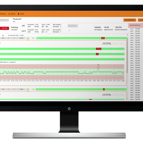
Recently, we had the pleasure of having James Guzzo from Impinj and Hannes Jehle from DELO present at our webinar on the intricacies of the RAIN RFID IC attach process. The webinar covered the numerous process variables that impact the quality and performance of the inlay, how IC manufacturing recipes can be used in the production process, and the critical role of process monitoring.
If you missed the webinar, the recording is available to view on-demand ›
Bonus Q&A – Questions Not Answered During the Live Session
The webinar topic proved to be a popular one. The presenters received so many questions during the webinar that the time ran out to cover all of them. So, we followed up with Hannes and James with a few of the questions that were not answered during the live session.
(I recommend you watch the webinar recording before reading the rest of this blog.)
Q1: How do we ensure the accuracy of IC positioning in the process?
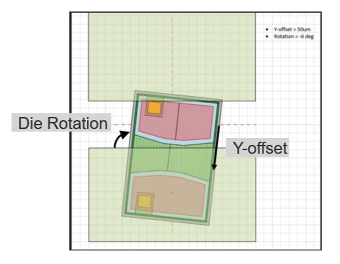
James Guzzo: The single biggest way that you can ensure the accuracy of the IC position is to turn on the DDA Vision system statistics (postplace.rep) and monitor the machine die ejection accuracy and adjust the DDA settings to improve the die ejection/placement accuracy if needed. There are two key parameters the DDA reports on which are the Y-offset (measured in microns) which is the shift up or down of the IC relative to the antenna gap. The second parameter is the die rotation left or right relative to a perfect alignment to the antenna gap (measured in degrees).

The Inlay assembly process allows for a certain level of inaccuracy in the Y-offset and Die rotation and will still produce a reliable, electrically well-performing inlay. The amount of Y-offset and die rotation tolerable is a function of the actual measured (actual) antenna gap and the size of the IC and the size of the IC pads.
There is the possibility that the die can shift or spin in the epoxy dot post-vision system inspection, but we have found the dominant factor in die placement accuracy occurs during die ejection off of the tape. The Voyantic Tagsuance inline electrical test yield generally correlates well with the postplace.rep placement accuracy.
Factors that impact the die placement accuracy and can be tuned to improve die placement: Die Ejector Needle Selection (needle tip radius and angle), dicing tape expansion, DDA die Ejection parameters(Cap Gap, Cap Retract, needle offset, vacuum delay,…)
Q2: Do you have any suggestions about the shape and also size of the die landing area? And what about the gap, previously you shoved 150um for the M800 series (talking about a “standard” antenna).
James Guzzo: See the response to Question 1 above for Context.
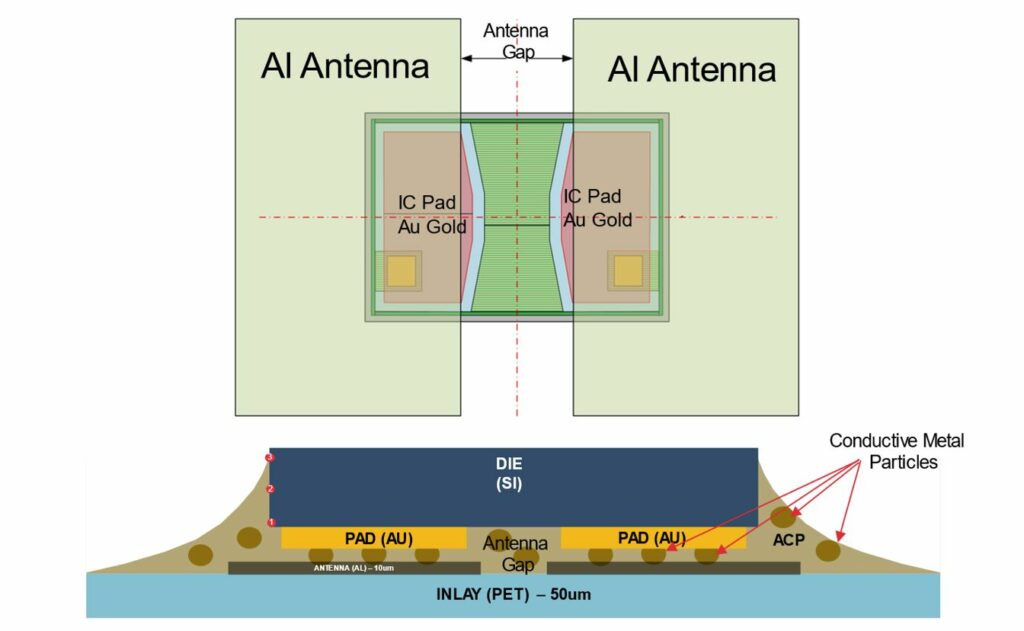
Ways to improve the maximum placement tolerance: Reduce the actual antenna gap of your antenna design by reducing your drawn antenna gap. Previously most etched Al on PET inlay manufacturers allowed a minimum drawn 140um and the stated actual gap tolerance is +/-50ums to the drawn. However many manufacturers typically do better than this and are closer to a +40um/-30 based on sampling and measuring actual antenna gaps for several models of inlays.
Numerous etched Al antenna on PET manufacturers now allow a minimum drawn antenna gap of 110um-120um drawn gap and correspondingly are able to achieve actual(measured) antenna gaps of 130um – 160um depending upon the antenna layout and geometries.
Q3: There is much recent talk or hype of “trillions” of RAIN RFID inlays per year to be made, presumably requiring thousands of chip-attach machines. What is the hourly capacity of the highest-capacity IC placement machine?
James Guzzo: The current state-of-the-art direct die attach machine models can create 40k, 80k, and up to 100k inlays per hour.
Q4: What is the allowed residue thickness between the gold pad and the aluminium for a proper connection – the thickness the gold particles can bridge?
James Guzzo: The electrical connection between the Tag ICs gold pads and the etched Aluminum Antenna Leads are actually made through the 3-8um diameter metal particles that are in the ACP (Anisotropic Conductive Paste). Different ACPs have different size particles of different conductive materials (e.g. tungsten, nickel, etc.) When the IC is bonded there are two hot pieces of metal in the Die attach machine (Called thermodes) that press against the back side of the die (from the top) and the bottom of the PET inlay. The thermodes accomplish 2 goals: The first is to push the conductive metal fragments into the gold pads and the Al antenna leads and the second goal is to cure or harden the Epoxy. One of the “Bonding” parameters is how much force the thermodes push the die into the inlay. The typical Thermode Bond Force is 1.5 Newtons to 2.5 Newtons.

Q4: Are there any low or no-heat adhesives being developed to save time and increase system throughput?
Hannes Jehle: At the moment heat curing is the only curing technology which allows the required reliability. There is a special “low temperature curing” adhesive in our portfolio which allows curing temperatures of 150°C.
Q5: Where do you see the company Delo’s glues in comparison to other glue manufacturers in the race for market share with next-generation machines driving the bonding times lower and temperature higher to reduce machine footprint?
Hannes Jehle: Besides many other applications I do see DELO as the leading supplier for ACAs for RFID applications. Due to our very fast development cycles, outstanding lab support, and very close cooperation with our partners. As far as I know, there are none or not many other ACA manufacturers that can make curing speeds of <100ms happen.
Q6: In your pictures, there is a lot of epoxy placed for those M700 chips. How do you avoid the chips being pulled up by the bond tape in the final bonder?
Hannes Jehle: The coating of the bond tape prevents the tape itself from sticking to the die or epoxy.
Q7: What will happen to an RFID tag if the ACP is not fully cured? Or if the bonding force is not enough or too much?
Hannes Jehle: The required reliabilities will not be achieved. (THT, bending, die shear)
——————————————————————–
See you at our next webinar!
All blog posts


