All blog posts

On-Demand Webinar – Achieving Excellence in RAIN RFID IC Attach Process

Feb 26, 2024

Recently, we had the pleasure of having James Guzzo from Impinj and Hannes Jehle from DELO present at our webinar on the intricacies of the RAIN RFID IC attach process. The webinar covered the numerous process variables that impact the quality and performance of the inlay, how IC manufacturing recipes can be used in the production process, and the critical role of process monitoring.

If you missed the webinar, the recording is available to view on-demand ›

Bonus Q&A – Questions Not Answered During the Live Session

The webinar topic proved to be a popular one. The presenters received so many questions during the webinar that the time ran out to cover all of them. So, we followed up with Hannes and James with a few of the questions that were not answered during the live session.

(I recommend you watch the webinar recording before reading the rest of this blog.)

Webinar Recording

Q1: How do we ensure the accuracy of IC positioning in the process?

James Guzzo: The single biggest way that you can ensure the accuracy of the IC position is to turn on the DDA Vision system statistics (postplace.rep) and monitor the machine die ejection accuracy and adjust the DDA settings to improve the die ejection/placement accuracy if needed. There are two key parameters the DDA reports on which are the Y-offset (measured in microns) which is the shift up or down of the IC relative to the antenna gap. The second parameter is the die rotation left or right relative to a perfect alignment to the antenna gap (measured in degrees).

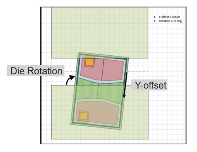
The Inlay assembly process allows for a certain level of inaccuracy in the Y-offset and Die rotation and will still produce a reliable, electrically well-performing inlay.  The amount of Y-offset and die rotation tolerable is a function of the actual measured (actual) antenna gap and the size of the IC and the size of the IC pads.

There is the possibility that the die can shift or spin in the epoxy dot post-vision system inspection, but we have found the dominant factor in die placement accuracy occurs during die ejection off of the tape.  The Voyantic Tagsuance inline electrical test yield generally correlates well with the postplace.rep placement accuracy.

Factors that impact the die placement accuracy and can be tuned to improve die placement: Die Ejector Needle Selection (needle tip radius and angle), dicing tape expansion, DDA die Ejection parameters(Cap Gap, Cap Retract, needle offset, vacuum delay,…)

Q2: Do you have any suggestions about the shape and also size of the die landing area? And what about the gap, previously you shoved 150um for the M800 series (talking about a “standard” antenna).

James Guzzo: See the response to Question 1 above for Context.

Ways to improve the maximum placement tolerance:  Reduce the actual antenna gap of your antenna design by reducing your drawn antenna gap. Previously most etched Al on PET inlay manufacturers allowed a minimum drawn 140um and the stated actual gap tolerance is +/-50ums to the drawn. However many manufacturers typically do better than this and are closer to a +40um/-30 based on sampling and measuring actual antenna gaps for several models of inlays.

Numerous etched Al antenna on PET manufacturers now allow a minimum drawn antenna gap of 110um-120um drawn gap and correspondingly are able to achieve actual(measured) antenna gaps of 130um – 160um depending upon the antenna layout and geometries.

Q3: There is much recent talk or hype of “trillions” of RAIN RFID inlays per year to be made, presumably requiring thousands of chip-attach machines. What is the hourly capacity of the highest-capacity IC placement machine?

James Guzzo: The current state-of-the-art direct die attach machine models can create 40k, 80k, and up to 100k inlays per hour.

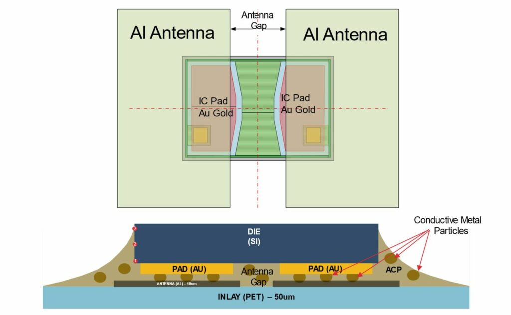
Q4: What is the allowed residue thickness between the gold pad and the aluminium for a proper connection – the thickness the gold particles can bridge?

James Guzzo: The electrical connection between the Tag ICs gold pads and the etched Aluminum Antenna Leads are actually made through the 3-8um diameter metal particles that are in the ACP (Anisotropic Conductive Paste). Different ACPs have different size particles of different conductive materials (e.g. tungsten, nickel, etc.) When the IC is bonded there are two hot pieces of metal in the Die attach machine (Called thermodes) that press against the back side of the die (from the top) and the bottom of the PET inlay. The thermodes accomplish 2 goals: The first is to push the conductive metal fragments into the gold pads and the Al antenna leads and the second goal is to cure or harden the Epoxy. One of the “Bonding” parameters is how much force the thermodes push the die into the inlay. The typical Thermode Bond Force is 1.5 Newtons to 2.5 Newtons.

Inlay bottom and cross-section view.

Q4: Are there any low or no-heat adhesives being developed to save time and increase system throughput?

Hannes Jehle: At the moment heat curing is the only curing technology which allows the required reliability. There is a special “low temperature curing” adhesive in our portfolio which allows curing temperatures of 150°C.

Q5: Where do you see the company Delo’s glues in comparison to other glue manufacturers in the race for market share with next-generation machines driving the bonding times lower and temperature higher to reduce machine footprint?

Hannes Jehle: Besides many other applications I do see DELO as the leading supplier for ACAs for RFID applications. Due to our very fast development cycles, outstanding lab support, and very close cooperation with our partners. As far as I know, there are none or not many other ACA manufacturers that can make curing speeds of <100ms happen.

Q6: In your pictures, there is a lot of epoxy placed for those M700 chips. How do you avoid the chips being pulled up by the bond tape in the final bonder?

Hannes Jehle: The coating of the bond tape prevents the tape itself from sticking to the die or epoxy.

Q7: What will happen to an RFID tag if the ACP is not fully cured? Or if the bonding force is not enough or too much?

Hannes Jehle: The required reliabilities will not be achieved. (THT, bending, die shear)

——————————————————————–

See you at our next webinar!

All blog posts
All blog posts

RAIN RFID Tag ICs – The Road to Configuration Words

Nov 21, 2023

Tag config memory –  What is that? Is it a fifth memory bank? Having configuration words in tag memory is the new normal in the industry and it is slowly gaining importance and cannot be ignored any longer. How did we end up with config words and how can we embrace them instead? Let’s take a look.  

Birth of Gen2

The core features and the operating principles of a RAIN tag IC have remained the same since the birth of the protocol in 2004 – The ability to wirelessly read and write memory contents, the ability to lock all or parts of the content from further edits by outsiders, and the ability to permanently disable the transponder when it has served its purpose.  That was pretty much it and to a great extent, still is.

The memory was organized into four parts all with their special purpose. Also, in the air interface protocol, a total of two bits were reserved to specify which memory was to be selected, read, written, or locked.

Memory bank 00 is the “reserved memory” and it contains the 32-bit Kill password as its two first words and the 32-bit Access password for the following two words, four 16-bit words in total.

Memory bank 01 is the “EPC memory”. This is where the EPC code is stored. EPC code is the specified part and length of the memory that will be broadcasted in the inventory process. The two first words in the EPC code have a special function. The very first word has a precalculated error correction word, CRC, stored in it. The second word, referred to as the protocol control word, or PC-word, is an important one. It is a word broadcasted prior to the EPC code in inventory and has several single-bit flags to tell which features tag has activated, and what numbering system it might belong to. It also has a 5-bit L parameter to tell and set the length of the broadcasted part of the EPC code. In short, in the inventory process, the tag would give a reply consisting of PC+EPC+CRC all from this memory.

Memory bank 10 is the “TID memory”. This has all the unalterable records of the tag locked from the factory in the wafer state. In particular, it has MDID specifying the company that designed the IC and TMN specifying the exact IC type and version.

Memory bank 11, is the “user memory”. This is a memory dedicated for the user to write any other entries the application needs, and should contain no special words or bits for the protocol or IC operation. As only a few applications require this type of “disc space” and most applications work solely around the EPC code, most commodity tags don’t actually have any user memory. Manufacturing expensive non-volatile memory “just in case” is too expensive as it uses quite a lot of  IC surface area.

Typical memory map and memory contents of the four memory banks when read with Tagformance Memory Management tool. The MDID+TMN reveal that this is the memory of a tag equipped with an older monza5 chip .

Rise and fall of the custom commands

Very soon after the very first wave of ICs had hit the market, the second wave of ICs from roughly 2010 and onward had several new features that were not considered in the original memory organization and protocol. However, the protocol had large RFU provisions for custom commands. So, each tag IC got their own set of special vendor and IC-specific commands to activate and control the new advanced features. The tag features were often clearly documented in datasheets and worked well. However, readers, their command sets, and UIs really struggled to keep up with new and specific firmware versions often needed. For practical matters, like controlling the privacy level of retail tags in this somewhat custom and vendor-specific way just didn’t work too well.

Gen2v2 to the rescue

In 2014, the protocol got a new version, the Gen2v2, which included many of the features added earlier as custom in a somewhat more standard way. The main topics that the new version touched were authentication, encryption, and user privileges. This cleaned the table a little, but still, using new commands to access new features was already found to not always be the easiest solution to adopt.

Configuration words

What happened nearly simultaneously with the release of Gen2v2 was that the control of these added features was slowly transferring from specific new commands to standard Select, Read, and Write commands just pointing to special memory locations. Every reader and reader UI already had filters and memory read functions enabled, so these could be “misused” to control tag settings. Specially formulated Select commands were used to trigger events like “record sensor reading” and “switch to temporary operating mode X”. Writing specific control bits changed settings like tag memory allocations and backscatter levels the state of which could be retained in memory from this point on and to be retained through power cycles.

Soon every manufacturer had their own “config memory bank” or “config word” hidden deep inside the already existing four banks with bits and parameters to be configured to tailor the tag functionality.  The trouble was that each IC manufacturer placed the config memory in a different place with varying functionality. Also changing the settings is not always as easy as hailing the tag and writing, as special safety measures are often set in place.

In hindsight, It would have been great to have had a 5th memory bank for tag settings, but as there were just the two bits in each command to specify the memory bank, we were already kind of maxed out at four.

Vendor-specific implementations

Impinj

From roughly the R6 family onwards, Impinj has chosen to place the config word in the reserved memory bank, right after the two passwords at address 0x04. This location has been kept throughout the various R6, M700, and M800 families of ICs with the purpose of each bit being kept more or less similar. Some of the features that can be configured are read range reduction, autotune disable, unkillable mode, and memory split between EPC and User memories, and some inventory optimization modes. More complex ICs like the Monza X-8K have used several words deeper in the same reserved bank for even more settings. Care must be taken when setting the features as only some of the bits can be written, some need to be written from a secured state with a non-zero access password and some bits can only ever be changed once. As the protocol only allows full 16-bit words to be written, changing single bits needs to be done with care and optimally the whole config set on one single write event.

A common reason for changing tag configuration is to trade some of the maximum EPC length into user memory. For instance, the only difference between the M830 and M850 is a different split between the EPC and user memory sizes, and the swap can also be made through the tag configuration bits.

NXP

NXP on the other hand has chosen to primarily use the word at a word address 0x20 in the EPC memory for configuration starting form the Ucode G2iL family of ICs and through the G2iM, Ucode 7, Ucode 8, and Ucode 9. Available features vary from model to model, some of them touching on the topics of product flags, backscatter strength and curve type,  parallel encoding, memory config selection, write power indicator, self-adjust settings, and memory checks. Some of the bits are action bits, meaning that selecting on those will trigger special features, some bits are permanent bits for configuring more permanent modes and some are purely indicator bits for reading current feature status. Changing some of the settings is careful work as some require a non-zero access password, then accessing the tag with that, then strictly using a mandatory Write command to perform a toggle-write on the bits that are wanted to be flipped.

NXP Ucode9 has config bits to select from different backscatter responses which can be helpful to optimize for privacy, performance, or conformance.

EM Microelectronic

EM Microelectronic has been known for their “more involved”, more advanced, and therefore also more complicated ICs hosting a variety of features, such as serial data interface, power outputs, sensoring, IO-pins, NFC+RAIN operation, TOTAL tag talks only modes, etc. These advanced settings often take several words of memory space for configuration in what EM refers to as “System memory” at the far end of the User memory bank.

Alien

Alien has a “Device configuration” often further up the TID memory bank. However, not many public datasheets are available describing the functionalities better. Most probably they are settings performed by the manufacturer and are not meant for the user or an encoding process to mess with. Anyhow, so far four manufacturers and four different memory banks have been chosen for config purposes.

Other manufacturers

With several dozens of Gen2 tag IC manufacturers in the game, there are too many to mention and not all distribute proper open datasheets to share all features in public. However, it seems that some of the newer players on the market have chosen to adopt one of the existing strategies, such as the Impinj Reserved memory word 0x04 for a comparable configuration. This might help existing readers support the newcomers when the location of the settings is the same.

Afterthoughts

There are several good aspects on this topic. First of all, for at least 90% of the customers, the initial settings are just fine. Also, with the two biggest RAIN IC providers on the market covering such a large market share, there nearly are two “standard” ways to control tag configurations. Furthermore, the Gen2v3 is just around the corner (more on that later), but it is not going to touch on the subjects typically controlled by the tag config bits. Unfortunate, that it will not clean this up, but then again fortunate, that it will not introduce even more ways to facilitate configurations that are bound to evolve faster than the protocol versions ever will. The place where the spread and complexity of configuring RAIN tags is putting the most pressure is probably in the encoding of tags where each IC type needs to be recognized and catered for to serve the remaining sub 10% of cases. If your software or UI is not recognizing the IC types, then the datasheet is your friend in deciphering the tag configuration options.

A personal plea to all the RAIN IC manufacturers out there: Please keep the datasheets publicly available to your customers and solutions providers. Also, luckily we are today talking about small single-bit differences in tag configs, as RAIN stands technologically relatively united and nowhere near as spread out and as complicated a disorder as the 13.56MHz playground that NFC is trying to unite and clean up. Let’s continue keeping RAIN united.

All blog posts
All blog posts

Switching into a New IC in Inlay Design – Is There a “Quick n’ Dirty” Way?

Jul 01, 2021

A few months ago, I started receiving questions about switching to a new IC in inlay manufacturing. All these vendors had done several IC changes over the years, but there was something new going on. The questions were centered around possible shortcuts in the process.

  • “What if I just change the IC and don’t change the antenna design at all?”
  • “What if I don’t waste time in machine settings and just do it quick n’ dirty?”
  • “Are there any ICs that are ‘plug and play’ with other models?”

Unfortunately, I could not offer any help. I did find the question interesting though. At first, I tried to figure out some approaches on my own but did not get past the very basics. That is when I asked help from my colleagues Juho Partanen and Jesse Tuominen, and started doing some research on the topic.

In scale comparison of Impinj M750 and Monza R6

Together with Juho and Jesse we put together a whitepaper that outlines the process and key considerations for switching from one IC to another.

Download the white paper

Key considerations for switching from one IC to another

The IC vendors have plenty of helpful material available:

  • IC Datasheets
  • Reference antenna designs
  • Industrialization guides.

Some of the material is not publicly available, so reaching out to the IC vendor for help is a good starting point.

  • Start by verifying the suitability of the IC functionality.
    If you only need 96bit EPC pretty much any IC can do it. But some IC’s have a lot more functionality. More EPC memory, different amounts of user memory, and they support various optional EPC gen2 commands.
  • Then focus on production.
    Getting all the details and settings in the IC attachment process adjusted for the new wafer, for the new IC, and possibly for the new bonding paste can take time. This is also a time to check the durability of the new IC attachment.
  • When the production compatibility is confirmed, focus on the antenna design.
    Optimizing antenna design is always recommended, and with the IC vendor’s reference designs as a starting point, the design is not that huge of a project. In some cases, it is possible to take small shortcuts, but the time saved is not much. A good and optimized design is a better approach.
  • Focus on quality.
    As with designs, shortcuts do not make sense. The best approach is to fully utilize the new IC and optimize the tag performance and quality.

Learn How to Switch from One RAIN RFID IC to Another

Learn more about each step in the process of switching from one IC to another

All blog posts